MBE-growth and studies 
   of MnF2 films on Si(111) and Si(001).
Motivation and methods
Main properties of MnF2 and CdF2 crystals
MBE growth of MnF2-CdF2 epitaxial layers
RHEED monitoring of SL growth
Double crystal X-ray diffractometry 
Photoluminescence of annealed MnF2/Si(111) structures
High Temperature Growth MnF2/Si(111)
AFM & RHEED images of annealed MnF2/CaF2/Si(111)
AFM & RHEED images of MnF2 layers on CaF2/Si(001)
Superlattice surface morphology
Summary
Main properties of MnF2 and CdF2 crystals


  • Insulators with energy band gap of 9 eV and 8 eV respectively
  • CdF2 shallow donor states with 0.1 eV activation energy and free electron concentration up to 1019cm-3
  • 3 eV conduction band offset at CdF2/ MnF2 interface
  • Antiferromagnetic ordering in MnF2 below 67.3 K
  • MnF2 tetragonal rutile-type phase (a=4.87A,c=3.31A) and several other phases at high pressure and temperatures
  • CdF2 cubic fluorite-type phase (a=5.39A)
  • Relatively small lattice mismatch (2.2%) for MnF2 and CdF2 cubic fluorite-type phases
  • The same signs of mismatch and lattice parameters close to Si for MnF2 and CdF2 fluorite-type phases
(D a/a) MnF2 = - 3.0%, (D a/a) CdF2 = - 0.8%


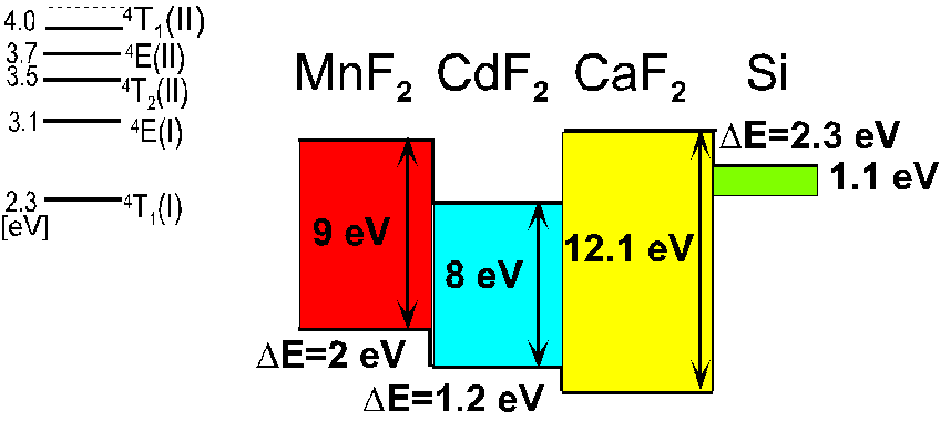
Fig. 1  Rutile MnF2crystal structure (above). Below  is the crystal structure of the orthorhombic a-PbO2 structure that stabilises in epitaxial growth on <111> Si substrates.
Fig. 2 Unit cell of rutile MnF2 (above) 


Band diagram of MnF2-CdF2-CaF2 heterostructures on Si(111)


band diagram Mnf2-CdF2-CaF2-Si


Contact person: Nikolai S.Sokolov Tel.: ++7 (812) 247-6411 Fax: ++7 (812) 247-1017;
e-mail: nsokolov@fl.ioffe.rssi.ru;

Web master: MarinaMoisseeva
e-mail: marina@fl.ioffe.rssi.ru;
 

Last revision: